[Gimp-user] PCB Editing
- From: Sorceress99 <forums gimpusers com>
- To: gimp-user-list gnome org
- Subject: [Gimp-user] PCB Editing
- Date: Fri, 17 Jan 2020 09:32:13 +0100
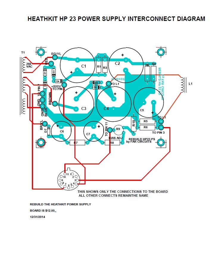
I am trying to separate the 2 sides of a printed circuit board photo and can't
remember how to do it.  The circuit diagram is in blue and the parts layout is
in black. Wiring placement is in red is irrevelant and can be deleted.  The PCB
pattern, in blue, is printed on glossy photo paper on a laser printer, in black.
The print is set on 'high quality' so needs to be sharp and clear. The image is
then positioned, face down on a blank copper clad PCB then transfered to the
board by various means such as heat lamination or chemically. Once completed,
the parts layout is printed on the laser as before, positioned in alignment with
the circuit side, then transfer to the opposite side of the board as before. Any
help with separating the 2 images would be appreciated.

Attachments:
* https://www.gimpusers.com/system/attachments/1338/original/HP-23_PCBFull.jpg

--
Sorceress99 (via www.gimpusers.com/forums)
[
Date Prev][
Date Next] [
Thread Prev][
Thread Next]
[
Thread Index]
[
Date Index]
[
Author Index]
